- 您现在的位置:买卖IC网 > Sheet目录331 > IPTR-DSPBUILDER (Altera)DSP BUILDER SOFTWARE
�� �
�
�Chapter� 3:� Design� Rules� and� Procedures�
�3–9�
�Frequency� Design� Rules�
�For� Simulink� simulation,� all� DSP� Builder� blocks� (including� registered� DSP� Builder�
�blocks)� use� the� sampling� period� specified� in� the� Clock� block.� If� there� is� no� Clock� block�
�in� your� design,� the� DSP� Builder� blocks� use� a� sampling� frequency� of� 1.� You� can� use� the�
�Clock� block� to� change� the� Simulink� sample� period� and� the� hardware� clock� period.�
�Multiple� Clock� Domains�
�A� DSP� Builder� model� can� operate� using� multiple� Simulink� sampling� periods.� You� can�
�specify� the� clock� domain� in� some� DSP� Builder� block� sources,� such� as� the� Counter�
�block.� You� can� also� specify� the� clock� domain� in� DSP� Builder� rate� change� blocks� such�
�as� Tsamp� .�
�When� using� multiple� sampling� periods,� DSP� Builder� must� associate� each� sampling�
�period� to� a� physical� clock� domain� that� can� be� available� from� an� FPGA� PLL� or� a� clock�
�input� pin.� Therefore,� the� top-level� DSP� Builder� model� must� contain� DSP� Builder� rate�
�change� blocks� such� as� PLL� or� Clock_Derived� .�
�You� can� use� a� PLL� block� to� synthesize� additional� clock� signals� from� a� reference� clock�
�signal.� These� internal� clock� signals� are� multiples� of� the� system� clock� frequency.�
�f� Refer� to� “Using� the� PLL� Block”� on� page� 3–14� for� more� information.�
�If� your� design� contains� the� PLL� block,� Clock� or� Clock_Derived� blocks,� the� DSP� Builder�
�registered� blocks� operate� on� the� positive� edge� of� one� of� the� block’s� output� clocks.�
�1�
�You� must� set� a� variable-step� discrete� solver� in� Simulink� when� you� are� using� multiple�
�clock� domains.�
�To� ensure� a� proper� hardware� implementation� of� a� DSP� Builder� design� using� multiple�
�clock� domains,� consider� the� following� points:�
�■�
�Do� not� use� DSP� Builder� combinational� blocks� for� rate� transitions� to� ensure� that� the�
�behavior� of� the� DSP� Builder� Simulink� model� is� identical� to� the� generated� RTL�
�representation.�
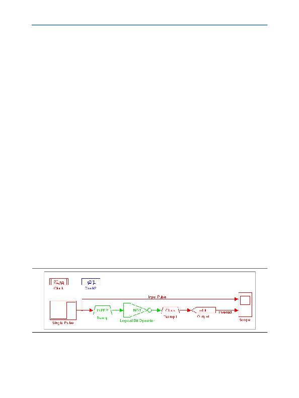
�Figure� 3–8� illustrates� an� incorrect� use� of� the� DSP� Builder� Logical� Bit� Operator�
�(NOT)� block.�
�Figure� 3–8.� Example� of� Incorrect� Usage:� Mixed� Sampling� Rate� on� a� NOT� Block�
�November� 2013�
�Altera� Corporation�
�DSP� Builder� Handbook�
�Volume� 2:� DSP� Builder� Standard� Blockset�
�发布紧急采购,3分钟左右您将得到回复。
相关PDF资料
IR11662SPBF
IC CNTROL SMART RECTIFIER 8-SOIC
IR1166STRPBF
IC MOSFET DRIVER N-CH 200V 8SOIC
IR11672ASPBF
IC MOSFET DRIVER 200V 8-SOIC
IR1167ASTRPBF
IC SMART SECONDARY DRIVER 8-SOIC
IR11682STRPBF
IC MOSFET DRIVER DUAL 200V 8SOIC
IR1168SPBF
IC MOSFET DRIVER DUAL 200V 8SOIC
IR1176STR
IC DRIVER RECT SYNC 5V 4A 20SSOP
IR2010SPBF
IC DRIVER HIGH/LOW SIDE 16SOIC
相关代理商/技术参数
IP-TRIETHERNET
功能描述:开发软件 Triple Spd Ethernet MegaCore
RoHS:否 制造商:Atollic Inc. 产品:Compilers/Debuggers 用于:ARM7, ARM9, Cortex-A, Cortex-M, Cortex-R Processors
IP-TRIETHERNETF
功能描述:开发软件 3x Spd Ethernet MAC MegaCore
RoHS:否 制造商:Atollic Inc. 产品:Compilers/Debuggers 用于:ARM7, ARM9, Cortex-A, Cortex-M, Cortex-R Processors
IPTV-OPTION-INS970
制造商:3M Electronic Products Division 功能描述:IPTV OPTION FOR INS970
IPU039N03L G
功能描述:MOSFET N-CH 30V 50A 3.9mOhms RoHS:否 制造商:STMicroelectronics 晶体管极性:N-Channel 汲极/源极击穿电压:650 V 闸/源击穿电压:25 V 漏极连续电流:130 A 电阻汲极/源极 RDS(导通):0.014 Ohms 配置:Single 最大工作温度: 安装风格:Through Hole 封装 / 箱体:Max247 封装:Tube
IPU039N03LG
制造商:INFINEON 制造商全称:Infineon Technologies AG 功能描述:OptiMOS?3 Power-Transistor Features Fast switching MOSFET for SMPS
IPU039N03LGXK
制造商:Infineon Technologies AG 功能描述:Trans MOSFET N-CH 30V 50A 3-Pin(3+Tab) TO-251
IPU04N03LA
功能描述:MOSFET N-CH 25V 50A IPAK RoHS:否 类别:分离式半导体产品 >> FET - 单 系列:OptiMOS™ 标准包装:1,000 系列:MESH OVERLAY™ FET 型:MOSFET N 通道,金属氧化物 FET 特点:逻辑电平门 漏极至源极电压(Vdss):200V 电流 - 连续漏极(Id) @ 25° C:18A 开态Rds(最大)@ Id, Vgs @ 25° C:180 毫欧 @ 9A,10V Id 时的 Vgs(th)(最大):4V @ 250µA 闸电荷(Qg) @ Vgs:72nC @ 10V 输入电容 (Ciss) @ Vds:1560pF @ 25V 功率 - 最大:40W 安装类型:通孔 封装/外壳:TO-220-3 整包 供应商设备封装:TO-220FP 包装:管件
IPU04N03LA G
功能描述:MOSFET N-CH 25V 50A IPAK RoHS:是 类别:分离式半导体产品 >> FET - 单 系列:OptiMOS™ 标准包装:1,000 系列:MESH OVERLAY™ FET 型:MOSFET N 通道,金属氧化物 FET 特点:逻辑电平门 漏极至源极电压(Vdss):200V 电流 - 连续漏极(Id) @ 25° C:18A 开态Rds(最大)@ Id, Vgs @ 25° C:180 毫欧 @ 9A,10V Id 时的 Vgs(th)(最大):4V @ 250µA 闸电荷(Qg) @ Vgs:72nC @ 10V 输入电容 (Ciss) @ Vds:1560pF @ 25V 功率 - 最大:40W 安装类型:通孔 封装/外壳:TO-220-3 整包 供应商设备封装:TO-220FP 包装:管件